
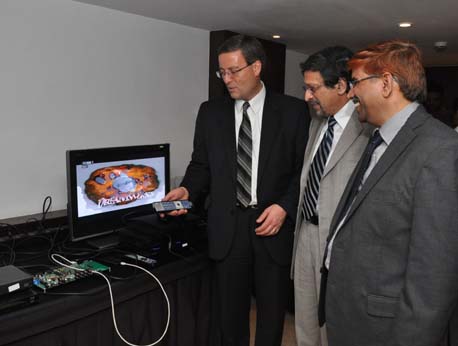
SUNNYVALE, Calif. and HYDERABAD, India, Feb. 17, 2012 – Leading US Silicon Valley-based provider of wireless and wired HD connectivity solutions, Silicon Image, formally opened its newest research and development (R&D) centre in India. Opened on January 27, 2012, the facility located in Hyderabad, focuses on the design and development of semiconductor and IP core technologies for implementation in mobile, wireless and consumer electronics (CE) products from manufacturers across the globe.
“The technology innovation and growth occurring in Hyderabad made the location a natural fit for Silicon Image’s expanding R&D portfolio,” said Rashid Osmani, vice president of worldwide engineering at Silicon Image, Inc. “The expertise of Silicon Image’s worldwide engineering team has been strengthened by the addition of the talented engineers in Hyderabad, who we foresee becoming an integral part of new product development.”
The Silicon Image India R&D center expands the company's current worldwide R&D operations which include facilities in Sunnyvale, CA, USA and Shanghai, China. The India office currently has 80 employees.
Silicon Image’s products are deployed by the world’s leading electronics manufacturers in devices such as desktop and notebook PCs, DTVs, Blu-ray Disc players, audio-video receivers, as well as mobile phones, tablets and digital cameras. Silicon Image has driven the creation of the highly successful HDMI and DV industry standards http://www.siliconimage.com/